IC DESIGN & PRODUCTION :: CONTRACT MANUFACTURING :: PRODUCT DEVELOPMENT
IC Services
To compliment our ASIC design services Sensonix has invested in developing full back-end wafer processing capabilities as well as packaging and test services. When wafers are received we typically have prototype devices ready for test within hours. In addition, Sensonix has full high volume production capbilities as well as inventory management services to support your production requirements.
Clean room class 10K Wafer probe test Wafer back grind Quick turn prototype packaging Laser mark High volume packaging and test Wafer bumping and bump wafer probe test Automated single die testing in production like quantities In house IC Packaging Ceramic Plastic Production off-shore packaging and test Life testing and burn in
RESOURCE CENTER

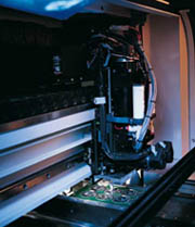
Our class 10,000 cleanroom facilitates the development of wafer-level and chip-level tests on site--eliminating outsourcing and maintaining control of this crucial aspect of processing.

Sensonix expertise includes ASIC finishing with solder bumps for flip chip or wafer-level chip scale packages (CSP). Wafer bumping can be processed with lead or lead free solder alloys. Contact