IC DESIGN & PRODUCTION :: CONTRACT MANUFACTURING :: PRODUCT DEVELOPMENT
Design Environment
Sensonix team can manage the entire IC development process from specification, design and fabrication through wafer processing, packaging and verification of engineering samples.
We begin by assisting with selection of the process technology that will best support your design and cost objectives. Design efforts will continue with detailed specification, architecture and partition planning, design entry, design verification, physical layout, and layout verification.
Sensonix will manage submission of the design directly to the foundry or IC fabrication service. Upon receipt of first wafers or bare die, Sensonix will handle all wafer processing and die packaging to deliver and test engineering samples.
Sensonix design environment is supported by commercial electronic design automation (EDA) tools to complete front-to-back IC design, engineering and production test facilities, and relationships with local independent IC consultants that can supplement our team with additional expertise.
RESOURCE CENTER
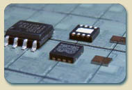
Beyond the IC, package selection and/or design is a key design aspect to be considered in preparing to deliver the component in volume production.